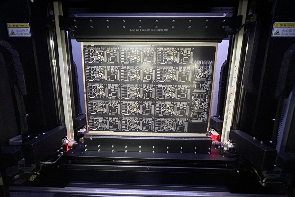
PCB proofing, that is, Printed Circuit Board (Printed Circuit Board, referred to as PCB) in mass production before the trial production stage, mainly used to determine the reliability of the PCB, processability and other related properties, to facilitate the subsequent need for mass production program. The following is a detailed explanation of PCB proofing:
I. Definition:
PCB proofing refers to the electronic engineers in the design of the circuit, and complete the drawing of the PCB, to the circuit board factory for small batch trial production process. Its main purpose is to verify the correctness of the design, feasibility and reliability, in order to find and solve potential problems before formal production.
Second, the sampling process:
Contact PCB board factory: first of all, you need to inform the PCB proofing factory of the design documents, process requirements, quantity and other information, so that the factory can provide quotations and subsequent production arrangements.
Cutting: According to the engineering information, cut out small production boards on the boards that meet the requirements.
Drilling: Drill the required holes on the cut boards according to the design requirements.
Copper Deposition: A thin layer of copper is chemically deposited on the walls of the insulating holes in preparation for subsequent graphic transfer.
Graphics Transfer: Transfer the image on the production film to the board to form the circuit pattern.
Pattern Plating: Plating a layer of copper or other metal of the required thickness on the exposed copper skin of the circuit pattern or on the wall of the holes to improve conductivity and durability.
Desmear: Use a specific solution to retire the anti-plating cover film layer, so that the non-line copper layer is exposed.
Etching: Using a chemical reaction to etch away the copper layer in the non-circuit area to form the final circuit pattern.
Green Oil: Coating a layer of green oil (solder resist) on a circuit board to protect the line and stop the line from being tinned when soldering parts.
Characters: Characters are printed on the circuit board for easy identification and marking.
Gold Plated Fingers: A nickel/gold layer is plated on the plug fingers to increase hardness and wear resistance.
Forming: Stamping through molds or CNC equipment to process the shape required by the customer.
Testing: Test the performance of the circuit board through electronic testing equipment to ensure that there are no defects such as open circuit and short circuit.
III. Precautions:
Size problem: In PCB proofing, the size must be in accordance with the requirements to avoid exceeding the actual production range.
Color issues: in the silkscreen color, you need to avoid the use of certain specific colors or concentrations of colors, so as not to be confused with the military standard.
Line problem: the thickness and density of the line need to meet the design requirements to ensure the performance and stability of the circuit board.
Soldermask type: according to the actual needs of the choice of the appropriate type of soldermask, such as tin spray, environmentally friendly soldermask and so on.
Fourth, there are obvious differences between PCB proofing and PCB production, these differences are mainly reflected in the following aspects:
1. Purpose and stage:
PCB proofing: mainly in the formal production before the production of a small number of samples for testing its performance, quality and manufacturability. Is a test and verification phase, the purpose is to ensure the correctness of the design and production feasibility.
PCB production: is in the above proofing verification through the premise of large-scale, batch production activities. The purpose of this stage is to meet market demand and provide stable and reliable products.
2. Quantity and scale:
PCB proofing: usually involves a small number of products, the number is small, mainly for testing and verification.
PCB production: involves a large number of products in large quantities to meet market supply and customer demand.
3. Processes and Stages:
Although both involve processes such as design, production and testing, the process of PCB proofing is more focused on verifying and modifying the design, while PCB production is more focused on large-scale, high-efficiency production.
4. quality requirements:
PCB proofing quality requirements are relatively high, PCB production quality requirements are stable and consistent.
PCB sampling quantity is small, the process is complex, the cost is relatively high. PCB production quantity is large, the process is standardized, the cost is relatively low.
6. Risks and problems:
PCB proofing: the main risk lies in the feasibility of design and manufacturing, the need to identify and solve potential problems.
PCB production: the main risk lies in the production process of quality control and cost control, the need to ensure product quality and reduce costs.
7. Usage and Scenario:
PCB sampling: mainly used for new product development, design verification, production feasibility testing and other scenarios.
PCB production: mainly used for large-scale, batch product supply to meet market demand.


