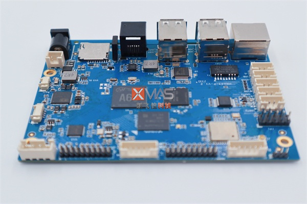
SMT SMD factory staff from the PCB sells not difficult to find the stacking design of most of the occasional layer rather than an odd number of layers, then, do you know these principles? Next we come together to talk about it:
In the manufacturing process circuit board conductive surfaces are precisely laid out on the core planes, these core planes usually use double-sided copper-clad substrate materials. When these core planes are fully utilized in the design, we will find that the number of conductive planes of the printed circuit board is always presented as an even number, when it comes to the cost of printed circuit boards (PCBs), although an odd number of layers of PCBs in the raw materials may seem to be more frugal, because it is one less layer of media and copper cladding layer, but in the actual production process, its cost will rise significantly. This is because odd-layer PCBs need to add an additional non-standard stacked core plane bonding process on top of the standard core plane structure process when manufacturing, which makes its processing cost much higher than single-layer PCBs, and even more than even-layer PCBs In addition, when we add copper cladding to the outside of the fiber core layer structure, it will lead to lower production efficiency and longer production cycle time, and also requires additional processing of the outer core plane before laminate bonding, all of which will result in lower production efficiency and longer production cycles. Additional processing is required before lamination bonding, all of which increases the risk of scratches and mismatches on the outer planes, which further pushes up the manufacturing cost. Therefore, an even number of PCBs is usually more advantageous from a total cost perspective.
In the design phase of the circuit board, if the number of stacked layers is odd, engineers can use some clever strategies:
1.SMT SMD factory's such as setting up a printed circuit board with an even number of power planes designed and an odd number of signal planes, an effective method is to increase the signal plane. This will not lead to increased costs, but can reduce processing time and improve the quality of the board.
2. SMT SMD assembly plus manufacturers of power supply layer for an odd number and the signal layer for an even number of times, you can add a power supply layer or without changing the other layout of the premise, in the middle of the stack to add a grounding layer to solve the problem.
3. For more complex microwave circuits and mixed dielectric circuits, the designer can also add a blank signal plane near the center of the PCB stack, thus reducing the stack imbalance.
Each project has its own unique needs and limitations, so the number of layers need to be selected according to the actual situation of flexible adjustment to ensure that the final product can meet the design requirements and have good performance.


