
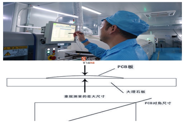
When a PCB (Printed Circuit Board) warps during production or use, it is like a subtle tilt in the cornerstone of a precision instrument. Although it may be difficult to detect with the naked eye, this non-planar deformation can cause a series of problems in the assembly process, posing a challenge to product quality and productivity. In this article, we will discuss with you the specific impact of PCB warpage on the assembly process.
First, SMT placement accuracy decline:
1.SMT (surface mount technology) is one of the core assembly means of modern electronics manufacturing industry, relying on the precise alignment of components and pads. When the PCB board is found to be warped problem, its surface no longer maintains the ideal flat state, directly affecting the SMT equipment placement effect.
2. Positioning deviation: Mounter relies on a high-precision vision system to identify the location of the pads to ensure that the components are accurately placed. Warped PCB will make the pad position relative to the vision system to produce offset, resulting in inaccurate placement of components.
3. Uneven pressure distribution: The pressure exerted by the mounter needs to be evenly distributed to ensure effective contact between components and solder paste. Warped PCB will make the mounting head and board contact pressure is uneven, may lead to component placement is not stable, or in the reflow soldering due to stress relief and displacement.
Welding defects: warpage caused by the pad and component terminals between the gap increases, may lead to inadequate filling of solder paste, the formation of cold welding or virtual welding, seriously affecting the reliability of the electrical connection.
Second, the wave soldering process problems highlighted:
For the use of through-hole plug-ins or hybrid process of PCB, warping problems in the wave soldering process should not be ignored:
1. Poor pad contact: warped PCB in the wave through the peak, part of the pad may not be able to fully contact with liquid solder, resulting in missing solder joints or insufficient solder, the formation of open or weak solder joints.
2. Welding stress and deformation aggravation: warped PCB in the wave soldering furnace when heated, due to the different coefficients of thermal expansion of the various parts, may further exacerbate the degree of warping or cause new deformation, not only affect the welding quality, but also may cause mechanical stress damage to the components.
Third, automated assembly and testing difficulties
1. Difficulty in automated plug-in: in the automatic plug-in machine, the warped PCB may lead to plug-in machine can not accurately align the jack, or in the insertion process of components and PCB caused unnecessary mechanical stress, and even lead to equipment damage.
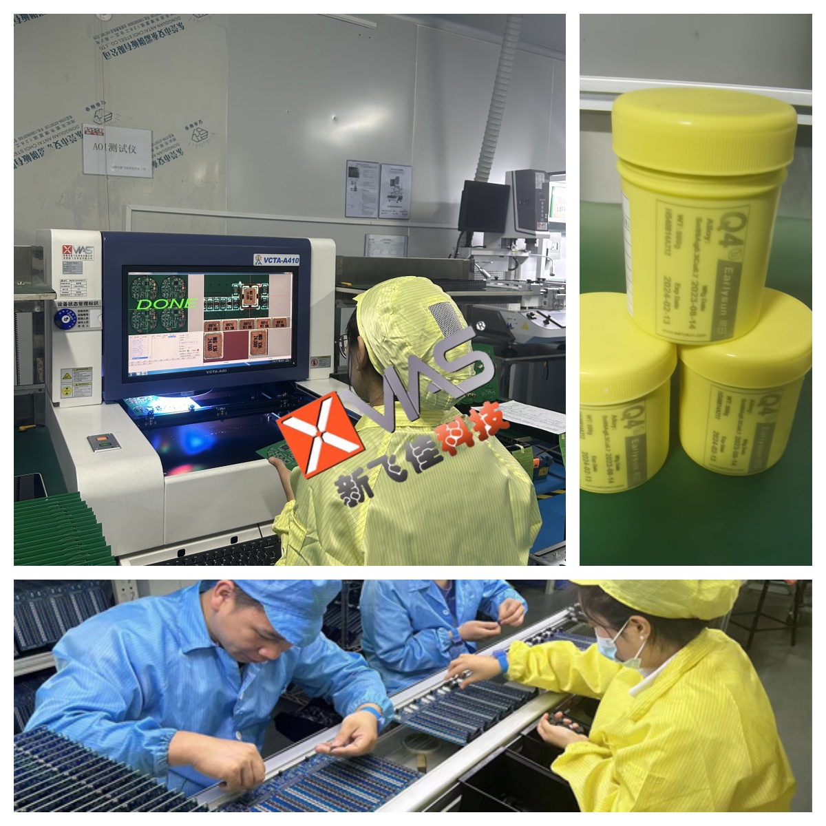
2. Reduced detection accuracy: AOI (Automated Optical Inspection, Automatic Optical Inspection) and AXI (Automated X-ray Inspection, Automated X-ray Inspection) system of imaging quality and detection accuracy affected by warpage, which may lead to defects missed or false alarms.
Fourth, mechanical assembly and heat dissipation performance is affected:
1. Increased assembly difficulty: warped PCB is difficult to be installed into the chassis or other hardware structure, may require additional manual adjustment or the use of auxiliary tools, increasing assembly time and cost, and may affect the overall stability of the final product.
2. Weakened thermal performance: warping leads to poor contact between the PCB and the heat sink or heatsink, hindering the effective conduction of heat, which may lead to overheating failures, affecting the long-term stable operation and service life of electronic equipment.
To summarize, PCB warpage has a wide and significant impact on the assembly process, affecting many key aspects such as SMT placement, wave soldering, automated assembly and testing, as well as final mechanical assembly and thermal management. Therefore, strict control of PCB warpage to ensure that it is within the allowable range is an indispensable quality control measure in the electronic manufacturing process.